- 您现在的位置:买卖IC网 > Sheet目录2007 > MAX1113CPE+ (Maxim Integrated Products)IC ADC 8BIT LP 16-DIP
A
MAX1112/MAX1113
+5V, Low-Power, Multi-Channel,
Serial 8-Bit ADCs
_______________________________________________________________________________________
3
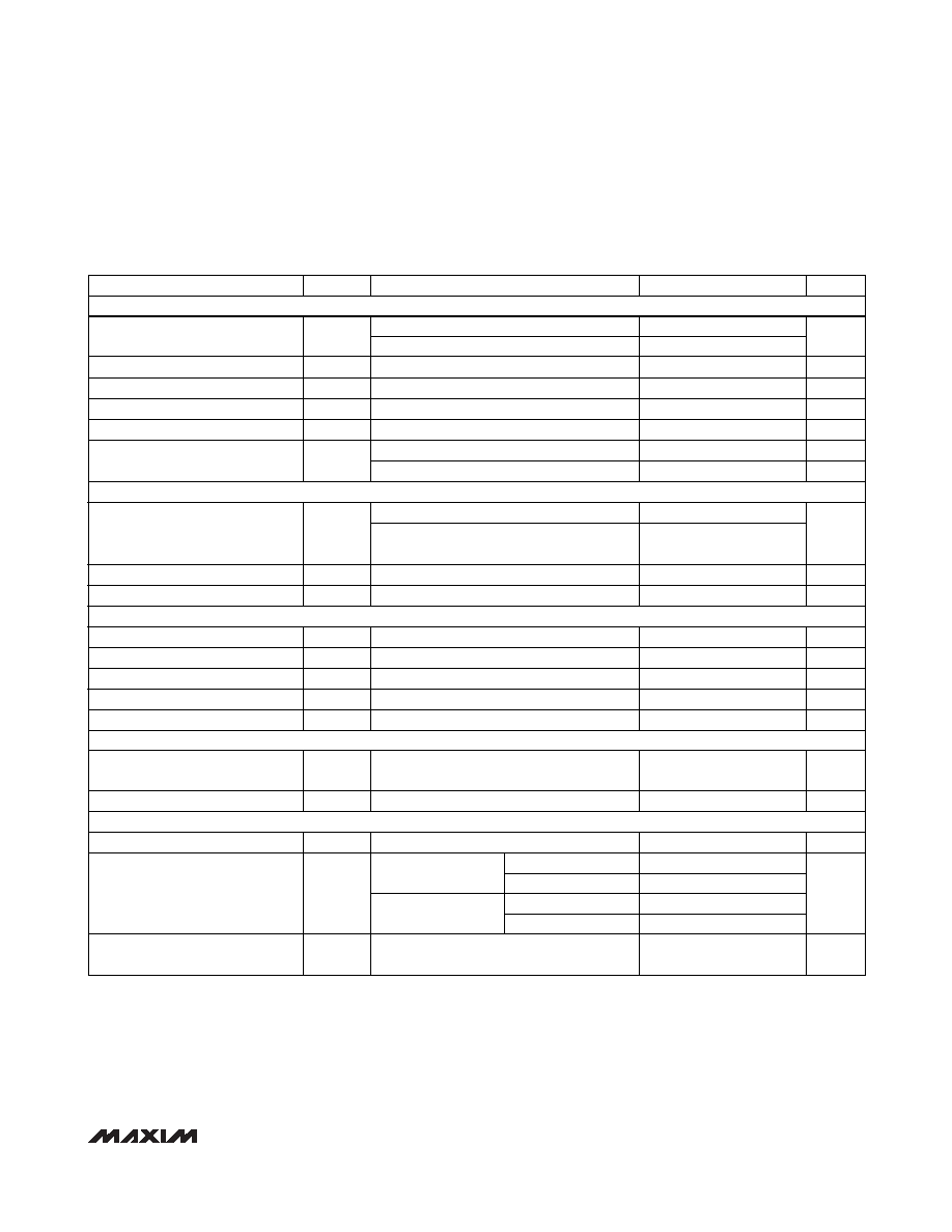
ELECTRICAL CHARACTERISTICS (continued)
(VDD = 4.5V to 5.5V; unipolar input mode; VCOM = 0V; fSCLK = 500kHz, external clock (50% duty cycle); 10 clocks/conversion cycle
(50ksps); 1F capacitor at REFOUT; TA = TMIN to TMAX; unless otherwise noted.)
On/off leakage current, VCH_ = 0V or VDD
Used for data transfer only
(Note 5)
External clock, 2MHz
CONDITIONS
ppm/°C
±50
mA
6
REFOUT Short-Circuit Current
pF
18
Input Capacitance
A
±0.01
±1
Multiplexer Leakage Current
1
2
50
500
kHz
400
Internal Clock Frequency
0 to 0.5mA output load
mV
4.5
Load Regulation (Note 7)
ns
10
Aperture Delay
s
1
tACQ
Track/Hold Acquisition Time
UNITS
MIN
TYP
MAX
SYMBOL
PARAMETER
ps
V
1
VDD +
50
Input Voltage Range
(Note 8)
A
120
Input Current
< 50
Aperture Jitter
External clock, 500kHz, 10 clocks/conversion
20
Internal clock
s
25
55
tCONV
Conversion Time (Note 4)
Bipolar input, VCOM = VREFIN/2
Unipolar input, VCOM = 0V
COM ±
VREFIN/2
V
0VREFIN
Input Voltage Range, Single-
Ended and Differential (Note 6)
V
3.936
4.096
4.256
REFOUT Voltage
External Clock-Frequency Range
MHz
kHz
Capacitive Bypass at REFOUT
F
REFOUT Temperature Coefficient
V
4.5
5.5
VDD
Supply Voltage
VDD = 4.5V to 5.5V; external reference,
4.096V; full-scale input
mV
±0.4
±4
PSR
Power-Supply Rejection
(Note 9)
2
Power-down
3.2
10
Software
SHDN at DGND
Operating mode
135
250
Full-scale input
CLOAD = 10pF
Reference disabled
95
IDD
A
Supply Current
CONVERSION RATE
ANALOG INPUT
INTERNAL REFERENCE
EXTERNAL REFERENCE AT REFIN
POWER REQUIREMENTS
发布紧急采购,3分钟左右您将得到回复。
相关PDF资料
MAX1116EKA+T
IC ADC 8BIT SERIAL SOT23-8
MAX11201BEUB+T
IC ADC 24BIT SRL 13.75SPS 10UMAX
MAX11202BEUB+T
IC ADC 24BIT SRL 13.75SPS 10UMAX
MAX11210EEE+T
ADC 24BIT 4WIRE SPI 16-QSOP
MAX11212BEUB+T
IC ADC 18BIT SRL 13.75SPS 10UMAX
MAX1135BCAP+
IC ADC 16BIT 150KSPS 20-SSOP
MAX1138LEEE+T
IC ADC 10BIT SERIAL 16-QSOP
MAX1159AEUI+
IC ADC 14BIT 135KSPS 28-TSSOP
相关代理商/技术参数
MAX1113EEE
功能描述:模数转换器 - ADC RoHS:否 制造商:Texas Instruments 通道数量:2 结构:Sigma-Delta 转换速率:125 SPs to 8 KSPs 分辨率:24 bit 输入类型:Differential 信噪比:107 dB 接口类型:SPI 工作电源电压:1.7 V to 3.6 V, 2.7 V to 5.25 V 最大工作温度:+ 85 C 安装风格:SMD/SMT 封装 / 箱体:VQFN-32
MAX1113EEE+
功能描述:模数转换器 - ADC 5V Low-Power Multi Ch Serial 8-Bit RoHS:否 制造商:Texas Instruments 通道数量:2 结构:Sigma-Delta 转换速率:125 SPs to 8 KSPs 分辨率:24 bit 输入类型:Differential 信噪比:107 dB 接口类型:SPI 工作电源电压:1.7 V to 3.6 V, 2.7 V to 5.25 V 最大工作温度:+ 85 C 安装风格:SMD/SMT 封装 / 箱体:VQFN-32
MAX1113EEE+T
功能描述:模数转换器 - ADC 5V Low-Power Multi Ch Serial 8-Bit RoHS:否 制造商:Texas Instruments 通道数量:2 结构:Sigma-Delta 转换速率:125 SPs to 8 KSPs 分辨率:24 bit 输入类型:Differential 信噪比:107 dB 接口类型:SPI 工作电源电压:1.7 V to 3.6 V, 2.7 V to 5.25 V 最大工作温度:+ 85 C 安装风格:SMD/SMT 封装 / 箱体:VQFN-32
MAX1113EEE-T
功能描述:模数转换器 - ADC RoHS:否 制造商:Texas Instruments 通道数量:2 结构:Sigma-Delta 转换速率:125 SPs to 8 KSPs 分辨率:24 bit 输入类型:Differential 信噪比:107 dB 接口类型:SPI 工作电源电压:1.7 V to 3.6 V, 2.7 V to 5.25 V 最大工作温度:+ 85 C 安装风格:SMD/SMT 封装 / 箱体:VQFN-32
MAX1113EPE
功能描述:模数转换器 - ADC RoHS:否 制造商:Texas Instruments 通道数量:2 结构:Sigma-Delta 转换速率:125 SPs to 8 KSPs 分辨率:24 bit 输入类型:Differential 信噪比:107 dB 接口类型:SPI 工作电源电压:1.7 V to 3.6 V, 2.7 V to 5.25 V 最大工作温度:+ 85 C 安装风格:SMD/SMT 封装 / 箱体:VQFN-32
MAX1113EPE+
功能描述:模数转换器 - ADC 5V Low-Power Multi Ch Serial 8-Bit RoHS:否 制造商:Texas Instruments 通道数量:2 结构:Sigma-Delta 转换速率:125 SPs to 8 KSPs 分辨率:24 bit 输入类型:Differential 信噪比:107 dB 接口类型:SPI 工作电源电压:1.7 V to 3.6 V, 2.7 V to 5.25 V 最大工作温度:+ 85 C 安装风格:SMD/SMT 封装 / 箱体:VQFN-32
MAX1113MJE
功能描述:模数转换器 - ADC
RoHS:否 制造商:Texas Instruments 通道数量:2 结构:Sigma-Delta 转换速率:125 SPs to 8 KSPs 分辨率:24 bit 输入类型:Differential 信噪比:107 dB 接口类型:SPI 工作电源电压:1.7 V to 3.6 V, 2.7 V to 5.25 V 最大工作温度:+ 85 C 安装风格:SMD/SMT 封装 / 箱体:VQFN-32
MAX1114
制造商:MAXIM 制造商全称:Maxim Integrated Products 功能描述:8-Bit, 150Msps Flash ADC